Applications
- Architectural glass
- Touch screens and flat monitors
- OLED applications
- Smart-glass applications
- Transparent antistatic foils
- Photovoltaic cells
- De-icing and heating applications
- Batteries
The EddyCus® TF map 2525SR and 5050SR are designed for contact-free real-time thickness and sheet resistance measurment of low and highly conductive thin films on glass, wafer, plastics or foils. The devices enable accurate and rapid high spatial resolution mapping of the sheet resistance of conductive films and the monitoring of metal film thickness. This non-contact mapping solution is beneficial for quality assurance for:
| Transparent Thin Films | Metallic Thin Films |
|---|---|
| Carbon Nano Tubes and Nano Buds | Aluminum |
| Graphene Films | Molybdenum |
| Metal Nano Wires | Silver |
| Nano Particle Films | Copper |
| and many more | and many more |
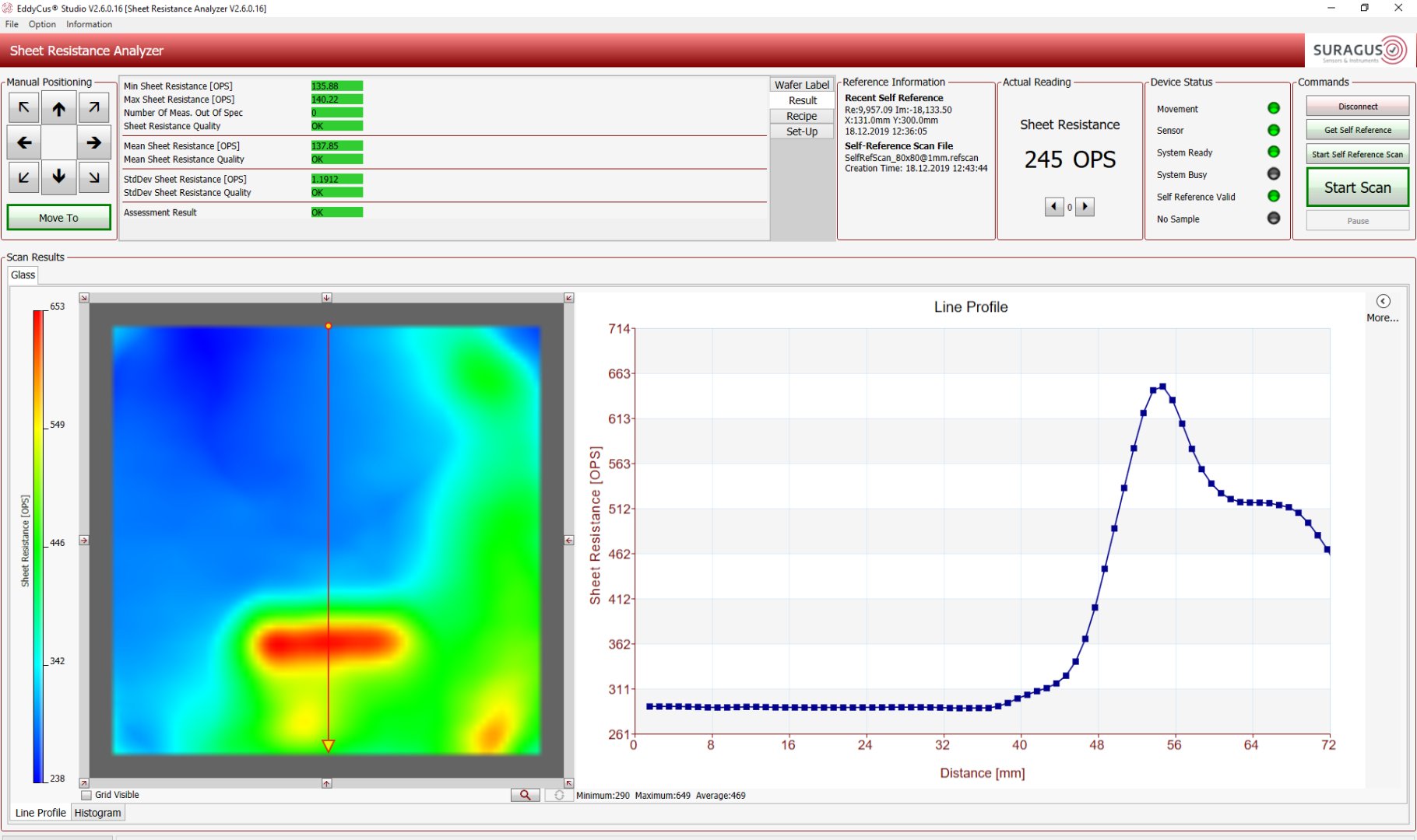
The Sheet Resistance Analyzer is a user-friendly program for system configuration and data review. The results of the testing processes are illustrated with graphical displays. Additional histograms and software tools enable a detailed sheet resistance measurement system.
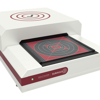
EddyCus® TF map 2525SR and 5050SR are gauges for fast mapping of sheet resistance, thickness, layer homogeneity, and conductivity effects and defects of conductive films and thin material systems on glass, wafer, and foils. There are different non-contact testing solutions available to suit different requirements.
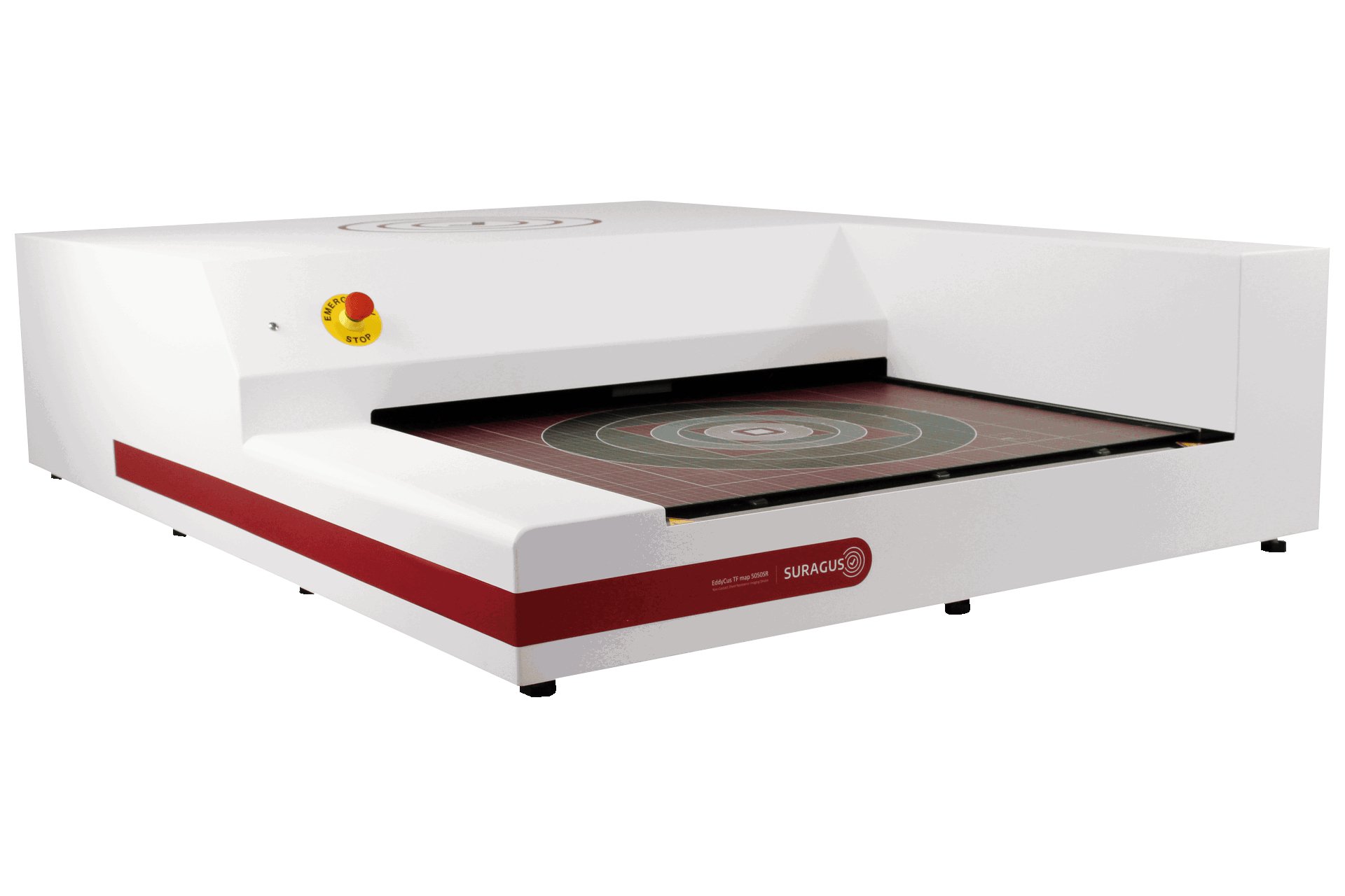
| EddyCus® TF map 2525 SR | EddyCus® TF map 5050 SR | |
|---|---|---|
| Sheet Resistance Measurement | Yes | |
| Thickness Measurement | Yes | |
| Optical Transmission | Optional | |
| Anisotropy Determination | Optional | |
| Sheet Resistance & Metal Thickness Measurement | Non-Contact Eddy Current Sensor | |
| Substrate Thickness Measurement | Ultrasonic Sensor | |
| Max. Scanning Area | 10 inch / 254 x 254 mm | 20 inch / 508 x 508 mm |
| Max. Sample Thickness (defines distances) |
2 / 5 / 10 / 14 mm (Defined by the thickest sample/application) |
|
| Sheet Resistance Range | 0.001 – 10 Ohm/sq; <2 % accuracy 10 – 100 Ohm/sq; < 3 % accuracy 100 – 1,000 Ohm/sq; < 5 % accuracy |
|
| Thickness Mapping of Metal Films (e.g. copper) | 2 nm - 2mm (in accordance with sheet resistance) |
|
| Scanning Time @ 1 - 10 mm Measurement Pitch | 4 inch / 100 x 100 mm in 0.5 to 5 minutes 8 inch / 200 x 200 mm in 1.5 to 15 minutes |
8 inch / 200 x 200 mm in 1.5 to 15 minutes 12 inch / 300 x 300 mm in 3 to 30 minutes |
| Scanning Pitch | 1 / 2 / 5 / 10 mm (other on request) | |
| Device Sizes (h/w/d) | 230 / 600 / 800 mm | 290 / 1180 / 900 mm |
| Weight | 27.0 kg | 120.0 kg |
| Available Features | Metal thickness tester Anisotropy sheet resistance sensor Optical transmission sensors at 632 nm wavelength |
|
REQUEST QUOTE